新闻资讯
联系我们
名 称:苏州赛森电子科技有限公司
电 话:0512-58987901
传 真:0512-58987201
邮 箱:sales@cycas.com
地 址:江苏省张家港经济开发区福新路1202号 215600PRC
网 址:www.cycas.com
Name: Suzhou cycas Microelectronics Co., Ltd.
Tel.: 0512-58987901
Fax: 0512-58987201
Email: sales@cycas.com
Address: No.1202,Fuxin Road,Zhangjiagang Economic Development Zone,Jiangsu Province 215600PRC
Website: www.cycas.com
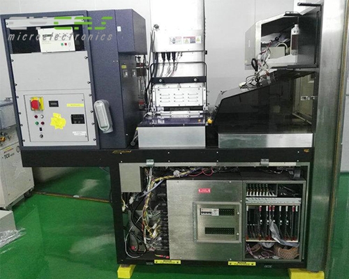
High density plasma etching is a key step in VLSI manufacturing高密度等离子体刻蚀是当今超大规模集成电路制造过程中的关键步骤
High density plasma etching is a key step in VLSI manufacturing高密度等离子体刻蚀是当今超大规模集成电路制造过程中的关键步骤
发布日期:2018-05-19 作者:www.cycas.com 点击:
高密度等离子刻蚀机是当今超大规模集成电路制造过程中的关键步骤。已经开发出许多终点检测技术,终点检测设备就是为实现刻蚀过程的实时监控而设计的。
光学发射
光学发射光谱法(OES)是使用最为广泛的终点检测手段。其原理是利用检测等离子体中某种反应性化学基团或挥发性基团所发射波长的光强的变化来实现终点检测。等离子体中的原子或分子被电子激发到激发态后,在返回到另一个能态时,伴随着这一过程所发射出来的光线。
光线的强度变化可从反应腔室侧壁上的观测孔进行观测。不同原子或分子所激发的光波波长各不相同,光线强度的变化反应出等离子体中原子或分子浓度的变化。被检测的波长可能会有两种变化趋式:一种是在刻蚀终点时, 反应物所发出的光线强度增加;另一种情形是光线强度减弱。

激光干涉
激光干涉终点法(IEP)是用激光光源检测透明薄膜厚度的变化,当厚度变化停止时,则意味着到达了刻蚀终点。其原理是当激光垂直入射薄膜表面时,在透明薄膜前被反射的光线与穿透该薄膜后被下层材料反射的光线相互干涉。
预报式检测
随着主流半导体工艺技术由0.18 μm 逐渐转移到0.13 μm工艺,以及最新的90 nm 工艺成功研发及投入使用。半导体器件的特征尺寸进一步减小,栅氧层的厚度越来越薄。90 nm工艺中,栅氧层的厚度仅为1.2 nm。如果等离子体刻蚀工艺控制不好, 则非常容易出现栅氧层的损伤;同时, 所使用的晶片尺寸增至300mm, 暴露在等离子体轰击下的被刻蚀面积不断缩小,所检测到的终点信号的强度下降,信号的信噪比降低。所有这些因素都对终点检测技术本身及其测量结果的可靠性提出了更加严格的要求。在0.18 μm工艺时,使用单一的OES检测手段就可满足工艺需求;进入0.13 μm 工艺后,就必须结合使用OES 及IEP 两种检测手段。由于IEP技术可以在刻蚀终点到达之前进行预报,因而被称为预报式终点检测技术。 [7]
High density plasma etcher is a key step in the manufacturing process of VLSI. Many end-point detection technologies have been developed, and the end-point detection equipment is designed to realize the real-time monitoring of the etching process. Optical emission
Optical emission spectrometry (OES) is the most widely used end-point detection method. The principle is to detect the end-point by detecting the change of the light intensity of the wavelength emitted by a reactive chemical group or volatile group in the plasma. When the atom or molecule in the plasma is excited to the excited state by the electron and returns to another energy state, it is accompanied by the light emitted by this process.
The change of light intensity can be observed from the observation hole on the side wall of the reaction chamber. The wavelength of the light wave excited by different atoms or molecules is different. The change of the light intensity reflects the change of the concentration of atoms or molecules in the plasma. There are two possible trends of the detected wavelength: one is that the light intensity of the reactant increases at the end of etching; the other is that the light intensity decreases.
Laser interference
Laser interference end-point method (IEP) uses a laser source to detect the thickness change of transparent film. When the thickness change stops, it means that the etching end-point is reached. The principle is that when the laser is perpendicular to the film surface, the reflected light in front of the transparent film interferes with the light reflected by the underlying material after penetrating the film.
Predictive detection
With the transition of the mainstream semiconductor technology from 0.18 μ m to 0.13 μ m, the latest 90 nm technology has been successfully developed and put into use. The characteristic dimensions of semiconductor devices are further reduced, and the thickness of gate oxide layer is becoming thinner. In the 90 nm process, the thickness of the gate oxide layer is only 1.2 nm. If the plasma etching process is not well controlled, it is very easy to damage the gate oxide layer; at the same time, the chip size used is increased to 300 mm, the etched area exposed to the plasma bombardment is continuously reduced, the intensity of the detected end-point signal is reduced, and the signal-to-noise ratio of the signal is reduced. All of these factors put forward more strict requirements for the end-point detection technology itself and the reliability of the measurement results. In the 0.18 μ m process, the use of a single oes detection method can meet the needs of the process; in the 0.13 μ m process, the use of oes and IEP must be combined. As IEP technology can predict the etching end-point before it arrives, it is called predictive end-point detection technology. [7]
本文网址:http://www.cycas.com/news/394.html
相关标签:等离子刻蚀机
最近浏览:
相关产品:
相关新闻:
- A complete set of equipment for surface modification, surface activation, etching and nano coating of plasma cleaning machine等离子体清洗机表面改性、表面活化、刻蚀、纳米涂层一台设备全搞定
- 等离子表面处理技术也具有以下优势Plasma surface treatment technology also has the following advantages
- 真空等离子清洗原理Principle of vacuum plasma cleaning
- 等离子清洗机在手机行业中的应用Application of plasma cleaning machine in mobile phone industry
- 真空等离子清洗产品特点Characteristics of vacuum plasma cleaning products
- 等离子体表面处理的原理Principle of plasma surface treatment
- 怎么选等离子清洗机设备厂商呢?How to choose plasma cleaning equipment manufacturers?
- 等离子清洗机效果如何评估 How to evaluate the effect of plasma cleaning machine?
- 等离子体表面处理的技术及应用Technology and application of plasma surface treatment
- A complete set of equipment for surface modification, surface activation, etching and nano coating of plasma cleaning machine等离子体清洗机表面改性、表面活化、刻蚀、纳米涂层一台设备全搞定 A complete set of equipment for surface modification, surface activation, etching and nano coating

