新闻资讯
联系我们
名 称:苏州赛森电子科技有限公司
电 话:0512-58987901
传 真:0512-58987201
邮 箱:sales@cycas.com
地 址:江苏省张家港经济开发区福新路1202号 215600PRC
网 址:www.cycas.com
Name: Suzhou cycas Microelectronics Co., Ltd.
Tel.: 0512-58987901
Fax: 0512-58987201
Email: sales@cycas.com
Address: No.1202,Fuxin Road,Zhangjiagang Economic Development Zone,Jiangsu Province 215600PRC
Website: www.cycas.com
Etching is one of the key technologies to determine the feature size刻蚀是决定特征尺寸的核心工艺技术之一
Etching is one of the key technologies to determine the feature size刻蚀是决定特征尺寸的核心工艺技术之一
发布日期:2018-02-01 作者:www.cycas.com 点击:
在众多半导体工艺中,刻蚀是决定特征尺寸的核心工艺技术之一。刻蚀分为湿法刻蚀和干法刻蚀。湿法刻蚀采用化学腐蚀进行,是传统的刻蚀工艺。它具有各向同性的缺点,即在刻蚀过程中不但有所需要的纵向刻蚀,也有不需要的横向刻蚀,因而精度差,线宽一般在3um以上。干法刻蚀是因大规模集成电路生产的需要而开发的精细加工技术,它具有各向异性特点,在最大限度上保证了纵向刻蚀,还可以控制横向刻蚀。本节介绍的硅等离子刻蚀机就是属于干法ICP(Inductively Coupled Plasma)刻蚀系统。它被广泛应用在微处理器(CPU)、存储(DRAM)和各种逻辑电路的制造中。
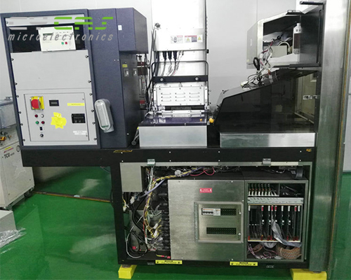
典型的硅刻蚀机系统结构如下图2-1所示。整个系统分为传输模块(Transfer Module)、工艺模块(Process Module)等。

图2-1 典型的硅刻蚀机系统结构 传输模块由Loadport、机械手(Robot)、硅片中心检测器等主要部件组成,其功能是完成硅片从硅片盒到PM的传输。Loadport用于装载硅片盒,机械手负责硅片的传入和传出。在传送过程中,中心检测器会自动检测硅片中心在机械手上的位置,进而补偿机械手伸展和旋转的步数以保证硅片被放置在PM静电卡盘的中心。 工艺模块(PM,如图2-2所示)是整个系统的核心,刻蚀工艺就在PM中完成。一个机台可以带2-4个工艺模块,工艺模块包括反应腔室、真空及压力控制系统、射频(RF)系统、静电卡盘和硅片温度控制系统、气体流量控制系统以及刻蚀终点检测系统等。其反应原理概述如下: 刻蚀气体(主要是F基和Cl基的气体)通过气体流量控制系统通入反应腔室,在高频电场(频率通常为13.56MHZ)作用下产生辉光放电,使气体分子或原子发生电离,形成“等离子体”(Plasma)。在等离子体中,包含由正离子(Ion+ )、负离子(Ion- )、游离基(Radical)和自由电子(e)。游离基在化学上很活波、它与被刻蚀的材料发生化学反应,生成能够由气流带走的挥发性化合物,从而实现化学刻蚀。另一方面,如图2-2所示,反应离子刻蚀腔室采用了阴极面积小,阳极面积大的不对称设计。在射频电源所产生的电场作用下带负电的自由电子因质量小,运动速度快,很快到达阴极;而正离子则由于质量大,速度慢不能在相同的时间内到达阴极,从而使阴极附近形成了带负电的鞘层电压。同时由于反应腔室的工作气压在10-3 ~10-2 Torr,这样正离子在阴极附近得到非常有效的加速,垂直轰击放置于阴极表面的硅片,这种离子轰击可大大加快表面的化学反应以及反应生产物的脱附,从而导致很高的刻蚀速率。正是由于离子轰击的存在才使得各向异性刻蚀得以实现。
In many semiconductor processes, etching is one of the key technologies to determine the feature size. Etching can be divided into wet etching and dry etching. Wet etching is a traditional etching process, which is carried out by chemical etching. It has the disadvantage of isotropy, that is, in the etching process, there are not only longitudinal etching but also transverse etching, so the accuracy is poor, and the linewidth is generally more than 3um. Dry etching is a fine machining technology developed for the needs of large-scale integrated circuit production. It has anisotropic characteristics, which ensures the maximum vertical etching and can also control the horizontal etching. The silicon plasma etching machine described in this section belongs to the dry ICP (inductively coupled plasma) etching system. It is widely used in the manufacture of microprocessor (CPU), memory (DRAM) and various logic circuits.
A typical silicon etcher system structure is shown in Figure 2-1. The whole system is divided into transfer module, process module and so on.
Figure 2-1 typical silicon etcher system structure transmission module is composed of loadport, robot, silicon center detector and other main components, whose function is to complete the transmission of silicon from silicon box to PM. Loadport is used to load the silicon box, and the manipulator is responsible for the incoming and outgoing silicon. During the transfer process, the center detector will automatically detect the position of the silicon center on the manipulator, and then compensate the extension and rotation steps of the manipulator to ensure that the silicon is placed in the center of the PM electrostatic chuck. The process module (PM, as shown in Figure 2-2) is the core of the whole system, and the etching process is completed in PM. One machine can be equipped with 2-4 process modules, including reaction chamber, vacuum and pressure control system, radio frequency (RF) system, electrostatic chuck and silicon chip temperature control system, gas flow control system and etching end point detection system. The reaction principle is summarized as follows: etching gas (mainly F-based and Cl based gas) is introduced into the reaction chamber through the gas flow control system, and glow discharge is generated under the action of high frequency electric field (frequency is usually 13.56MHz), which ionizes the gas molecules or atoms and forms plasma. The plasma consists of positive ion (ion +, negative ion (ion -), free radical and free electron (E). Free radicals are chemically active. They react with the etched material to form volatile compounds that can be removed by the air flow, thus achieving chemical etching. On the other hand, as shown in Figure 2-2, the reactive ion etching chamber adopts the asymmetric design with small cathode area and large anode area. Under the action of the electric field produced by the RF power supply, the negative free electron has small mass, fast moving speed, and quickly reaches the cathode; while the positive ion can not reach the cathode in the same time due to its large mass, so the negative sheath electric pressure is formed near the cathode. At the same time, the working pressure of the reaction chamber is in the range of 10-3 ~ 10-2 Torr, so that the positive ions can be accelerated very effectively near the cathode. The vertical bombardment can greatly accelerate the chemical reaction on the surface and the desorption of the reaction products, resulting in a high etching rate. It is the ion bombardment that makes anisotropic etching possible.
本文网址:http://www.cycas.com/news/382.html
相关标签:等离子刻蚀机
最近浏览:
相关产品:
相关新闻:
- 等离子体表面处理的原理Principle of plasma surface treatment
- 等离子表面处理技术也具有以下优势Plasma surface treatment technology also has the following advantages
- 等离子清洗机在手机行业中的应用Application of plasma cleaning machine in mobile phone industry
- A complete set of equipment for surface modification, surface activation, etching and nano coating of plasma cleaning machine等离子体清洗机表面改性、表面活化、刻蚀、纳米涂层一台设备全搞定 A complete set of equipment for surface modification, surface activation, etching and nano coating
- 真空等离子清洗产品特点Characteristics of vacuum plasma cleaning products
- 等离子体表面处理的技术及应用Technology and application of plasma surface treatment
- A complete set of equipment for surface modification, surface activation, etching and nano coating of plasma cleaning machine等离子体清洗机表面改性、表面活化、刻蚀、纳米涂层一台设备全搞定
- 真空等离子清洗原理Principle of vacuum plasma cleaning
- 等离子清洗机效果如何评估 How to evaluate the effect of plasma cleaning machine?
- 怎么选等离子清洗机设备厂商呢?How to choose plasma cleaning equipment manufacturers?

